Advancements in Semiconductor Packaging Technologies in the UK
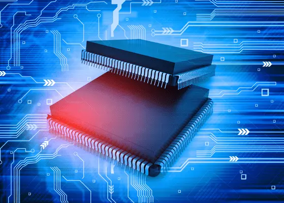
Semiconductor packaging is a vital stage in the chip manufacturing process that often goes unnoticed but plays a crucial role in determining the final device’s performance, size, and durability. In the United Kingdom, innovation centers, research organizations, and semiconductor firms are leading the way in developing new packaging technologies to address increasing demand for smaller, faster, and more efficient chips. These innovations are particularly significant as semiconductor products grow more complex, necessitating novel solutions for addressing the complications of power management, thermal dissipation, and integration density.
The packaging procedure involves safeguarding the semiconductor die, delivering electrical interfaces, and controlling heat dissipation. Conventional packaging methods are approaching their physical limits because contemporary chips contain billions of transistors, function at increased frequencies, and need to be housed in ever-smaller devices. The UK semiconductor industry is countering with innovative packaging technologies including three-dimensional (3D) packaging, system-in-package (SiP), and fan-out wafer-level packaging (FOWLP).
The Emergence of 3D Packaging and Heterogeneous Integration
One of the most disruptive trends in semiconductor packaging in the UK is 3D integration technology. In contrast to traditional two-dimensional architectures, 3D packaging stacks semiconductor dies vertically. Stacking minimizes the distance electrical signals must travel between devices, leading to enhanced speed, low power consumption, and increased signal integrity. These advantages are crucial to high-performance computing applications such as artificial intelligence (AI), data centers, and next-generation mobile devices.
Alongside this, the UK is aggressively pursuing heterogeneous integration, where various forms of chips are integrated into one package. This is conducive to multi-functional semiconductor modules that can have logic, memory, sensors, and power management components integrated together.
UK research institutions, including the National Microelectronics Centre and the Compound Semiconductor Applications Catapult, are leading the way in creating these new packaging technologies. These facilities make specialist equipment and expertise available to industry, enabling quick prototyping and testing of new packaging concepts.
Overcoming Thermal Management and Reliability Issues
As devices become more powerful and denser, heat dissipation in the package is more and more a priority. Excess heat detracts from chip performance and shortens the device life, so thermal management is a key factor in packaging design.
The UK semiconductor sector is pioneering the creation of thermal interface materials that enhance heat transfer from the chip. New cooling technologies, such as microfluidic channels incorporated into the package and advanced heat spreaders, are also being developed to ensure optimal working temperatures. All this promotes increased reliability and facilitates the manufacture of chips that can work efficiently under heavy loads.
In addition, robust testing and quality control are an essential part of the packaging process. UK companies are optimizing their reliability qualification methodologies to guarantee that high-end packages satisfy the stringent needs of industries like automotive and aerospace, where failure is unacceptable. These activities contribute to customer confidence and make UK semiconductor products popular around the world.
Collaborative R&D and Industry Partnerships
Development of semiconductor packaging in the UK is supported by close interaction between industry stakeholders, government, and academia. Government funding initiatives and public-private partnerships give the necessary funds to fund research and development activities.
Organizations such as Innovate UK and UK Research and Innovation (UKRI) actively fund projects that discover novel packaging materials, integration methods, and fabrication processes. These projects promote knowledge sharing and minimize the cost and time of deploying innovations from the lab to the marketplace.
Market Impact and Future Prospects
The reach of new packaging technologies goes beyond technical performance enhancement. Through the capability to produce smaller, faster, and lower-power chips, such advancements allow UK semiconductor companies to access high-growth applications like 5G infrastructure, electric vehicles, and wearable electronics.
For instance, the use of SiP and FOWLP technologies enables the integration of communication modules in IoT devices with minimal size, boosting connectivity and functionality.
In the future, the UK semiconductor packaging industry will continue to expand. Investments in pilot production lines, staff skill-building, and environmentally friendly manufacturing processes will aid in the ramp-up of these next-generation technologies. Ongoing emphasis on innovation and partnerships is likely to establish the UK as a core player within the global semiconductor value chain.
For in-depth information on UK semiconductor innovations, see our UK Semiconductor Market
Packaging Innovation as a Driver of UK Semiconductor Competitiveness
With the evolution of semiconductor technology, packaging innovation plays a progressively crucial role in providing high-performance, integrated solutions that capture the needs of contemporary applications. The UK's focus on developing and embracing sophisticated packaging methods such as 3D integration and heterogeneous systems puts its semiconductor industry on track for long-term growth and global competitiveness.
By continuing to push the boundaries in semiconductor packaging, the UK is shaping the future of electronics and securing its role in the evolving global technology landscape.


Share